YoWASP Puts a Yosys Toolchain Everywhere with the Power of WebAssembly
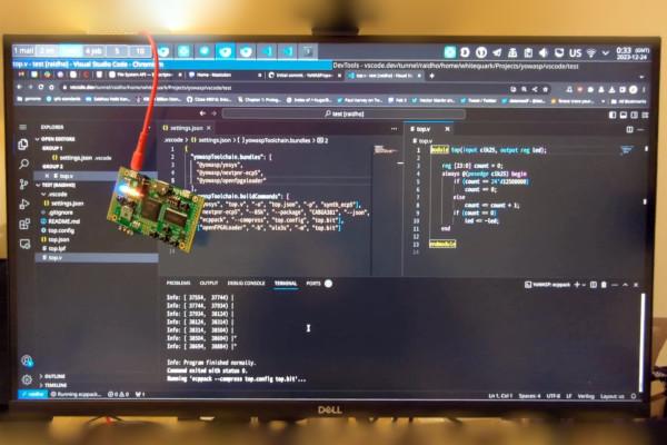
YoWASP, a FOSSi Foundation project, aims to put Yosys, the nextpnr place-and-route project, and more onto as many devices as possible with as low a barrier to entry as can be - by creating packages built in WebAssembly.
"I finally did it," Catherine "whitequark" writes of the project. A complete FPGA toolchain (synthesis, placement, routing, and programming) running entirely in the browser. The toolchain even works on my Pixel 6 (in Chrome). Has anyone ever programmed an FPGA from their mobile phone before?"
The YoWASP project takes existing open-source tools for FPGA development and creates packages based on WebAssembly and the WebAssembly System Interface - meaning not only that they can now run in-browser but that a single binary can run on multiple platforms and operating systems, with the initial release supporting Linux and Apple macOS on x86_64 and AArch64 platforms and Microsoft Windows on x86_64.
In addition to running in-browser, the resulting packages can be distributed using package managers designed for use with various programming languages like Python's PyPI and JavaScript's NPM. As a result, tools can be added as dependencies and have their versions frozen, among other useful features.
More details on the YoWASP project are available on the official website, while source code is published to GitHub; whitequark has also published a Microsoft VSCode extension for experimentation.
Leo Moser Pens an Introduction to Minimal Fab and the Open-Source ICPS PDK
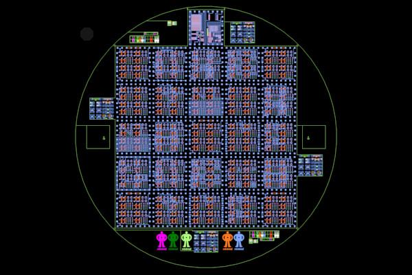
Leo Moser is looking to introduce people to the open-source ICPS Process Design Kit (PDK) with a step-by-step tutorial - starting with an introduction to the PDK and Minimal Fab.
"Recently I participated in the Minimal Fab Design Contest," Leo explains. "I had a go at designing a transmission-gate D-FF using the provided template for the layout. You could only use the first metal layer to connect devices. This was only possible because the Industrial CPS Research Center (ICPS) at AIST (Advanced Industrial Science and Technology) in Japan open sourced their PDK for the Minimal Fab SOI-CMOS process."
That open-source PDK was at the heart of the contest, which as the name implies focused on offering a minimal level of technology - with a "minimal fab" costing "only" tens of millions in facilities and equipment, compared to the billions required for a modern "megafab," and spitting out prototype chips in as little as 10 days based on standardised shuttles.
"The PDK is not only open source," Leo notes, "but it is also designed for open source tools. We will be using xschem for schematic entry, ngspice for simulation purposes and KLayout for the layout of the design."
For those who want to follow along, the introductory blog post and more detailed hands-on tutorial are both live on Leo's blog now.
Olimex Announces an Open-Source Dev Board for the Cologne Chip GateMate A1
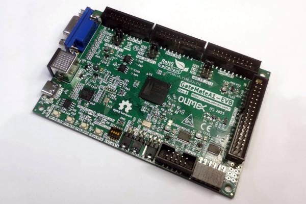
Bulgarian open hardware specialist Olimex is preparing to release a low-cost development board built around the Cologne Chip GateMate A1 - undercutting the official evaluation board without skimping on features.
"Cologne Chip is a European FPGA vendor," Olimex founder Tsvetan Usunov writes of his interest in the company's products. "Their GateMate A1 chip has nice features, but what we really like is their open source commitment - they offer open source tools for programming."
The GateMate CCGM1A1, or GateMate A1, is built around Cologne Chip's "Cologne Programmable Elements," or CPEs. Each chip has 20,480 CPEs, which can be configured as 20,480 eight-input LUT trees or 40,960 four-input LUT trees with 40.960 flip-flops or latches.
The Olimex GatemateA1-EVB, meanwhile, is an open hardware development board built around the GateMate A1 - delivering the FPGA itself, 64Mb of pseudo-static RAM (PSRAM), a Raspberry Pi RP2040 coprocessor for programming and debugging, and connectivity including VGA video and PS/2 keyboard, UEXT and PMOD, and four input/output banks with 1.2V, 1.8V, and 2.5V selectable logic levels.
At the time of writing, Olimex had received the first board prototypes and was going through the testing process ahead of general availability; the company aims to launch the boards soon at €50 each.
More information is available on the Olimex blog.
lowRISC Celebrates Milestones in an Update on the Sunburst Project
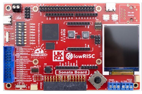
The Sunburst Project, which aims to enhance security in embedded and operational technology sectors through the adoption of the open-source CHERIoT microcontroller, has hit some major milestones - detailed by lowRISC in a project update.
"CHERIoT as a Microsoft-developed architecture extension brings CHERI features to the 32-bit RISC-V microcontroller domain, and Microsoft recently open-sourced a first, real-world implementation of it based on lowRISC’s popular Ibex CPU core," lowRISC explains, referring to the CHERI project to add hardware memory protection and compartmentalisation to processors.
"The Sunburst Project, in turn, was set up to leverage and popularize CHERIoT, by delivering a) a low-cost evaluation board hosting that baseline CHERIoT-Ibex implementation (codenamed '
'Sonata'); and b) a more fully-featured top-level design unifying the mature OpenTitan silicon root of trust with CHERIoT-Ibex (codenamed 'Symphony')."
Since its founding, the Sunburst Project has released architecture documentation for Sonata and Symphony, lowRISC explains, and schematics and design files for the Sonata board - under the permissive Apache 2.0 licence.
"In line with the project’s commitment to get usable CHERI technology into the hands of embedded system engineers," the organisation adds, "the Sunburst Project is preparing 100 of these prototype CHERIoT-Ibex Sonata boards for free distribution to qualifying institutions in the first half of 2024. A version of these prototype boards will also be made available commercially through distribution channels such as Mouser, making them accessible in higher volumes to a broader audience."
More details, including links to the documentation and Sonata design files, are available on the lowRISC blog.; additional information can be found on the Sunburst Project website.
"Clockhands" Promises Better Out-of-Order CPU Energy Efficiency
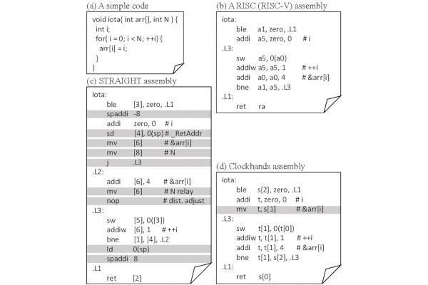
A team of researchers from the Nagoya Institute of Technology and the University of Tokyo have published a paper proposing a new instruction set architecture, Clockhands, which is claimed to offer major gains in energy efficiency for out-of-order processors - up to 24 per cent over a standard RISC architecture, they claim.
"Out-of-order superscalar processors are currently the only architecture that speeds up irregular programs, but they suffer from poor power efficiency," the researchers explain. "To tackle this issue, we focused on how to specify register operands. Specifying operands by register names, as conventional RISC does, requires register renaming, resulting in poor power efficiency and preventing an increase in the front-end width.
"We propose Clockhands, a novel instruction set architecture that has multiple register groups and specifies a value as 'the value written in this register group k times before.' We implemented a cycle-accurate simulator, FPGA implementation, and first-step compiler for Clockhands and evaluated benchmarks including SPEC CPU. On a machine with an eight-fetch width, the evaluation results showed that Clockhands consumes 7.4 per cent less energy than RISC while having performance comparable to RISC."
That energy-efficiency gain is impressive enough, and comes at the advantage over rival architecture STRAIGHT by requiring fewer extra instructions over conventional RISC architectures, but the team promises more: "This energy reduction increases significantly to 24.4 per cent when simulating a futuristic up-scaled processor with a 16-fetch width," they write, "which shows that Clockhands enables a wider front-end."
The team's full paper has been published under open-access terms in the Proceedings of the 56th Annual IEEE/ACM International Symposium on Microarchitecture.
BSC Presents Sargantana, a "New Generation" of Spanish Open-Source Silicon
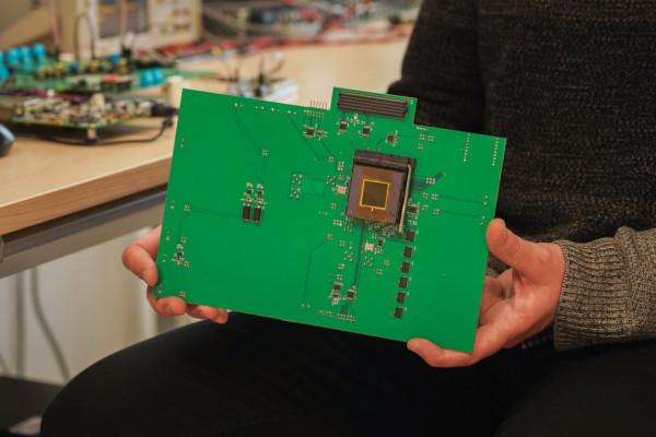
The Barcelona Supercomputing Centre (BSC) has unveiled a third-generation entry in its in-house Lagarto processor family, subbed Sargantana - part of the Designing RISC-V Accelerators for Next-Generation Computers (DRAC) project.
"The launch of Sargantana is a further step forward in the development of European RISC-V based technology, an embryo of the future European high-performance processor," claims BSC director Mateo Valero of the release. "This open hardware will be vital to ensure technological sovereignty and maintain European industrial competitiveness, and consolidates the BSC's role as a pioneer in Europe in the introduction of open source for chip design.
"We have the talent, the technological knowledge and the scientific environment necessary for Barcelona and its surroundings to be able to compete with any institution or region in the world and become a 'Design Valley' that drives the creation of companies and new jobs."
The Sargantana is an RV64G RISC-V design which follows on from the project's earlier Lagarto Hun and DVINO designs, released in 2019 and 2021 respectively, and comes as the first Lagarto chip to break the 1GHz frequency barrier - hitting 1.26GHz in the "slow corner" and up to 1.69GHz at its fastest using 22nm FD-SOI fabrication.
Sargantana is available on GitHub under the permissive Solderpad Hardware License v2.1.
 g)
g)
Matt Venn Takes a Look at How Chips are Made at IHP
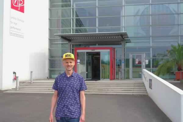
Matt Venn, of the Zero to ASIC Course, has published a video tour showing how chips are made at the Leibniz Institute for High Performance Microelectronics (IHP) - showcasing what happens after designs made in the IHP open-source Process Design Kit (PDK) are submitted for manufacture.
Part of Matt's educational video series, which supports the hands-on Zero to ASIC Course and Tiny Tapeout programmes, the tour goes through the full process: entering the cleanroom, cleaning and treating the silicon wafers, the photolithographic process, wafer indexing, chemical vapour deposition, ion implantation, annealing, and more - everything that turns a silicon wafer into working chips, bar the packaging.
"It's very rare to get a look inside a foundry, and that's because the semiconductor industry doesn't want to share its expensive secrets," Matt opines. "As well as IHP letting us look inside their factory they're also letting us look inside their PDK - that's the library of all the things you need to know to actually design a chip.
"They're part of a growing movement that's making semiconductors more accessible to everyone. In 2024, IHP plans to let amateurs like you and more get our chips made here."
The full video is available on the Zero to ASIC Course YouTube channel.
Upcycled REFRESH FPGAs Aim to Make Technology More Sustainable
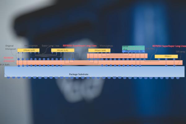
Researchers from the University of Notre Dame and the University of Pittsburgh have detailed a new approach to FPGA development: upcycling "recently retired" FPGA dies into "new" devices.
"There is a growing call for greater amounts of increasingly agile computational power for edge and cloud infrastructure to serve the computationally complex needs of ubiquitous computing devices. Thus, an important challenge is addressing the holistic environmental impacts of these next-generation computing systems," the team explains. "To accomplish this, a life-cycle view of sustainability for computing advancements is necessary to reduce environmental impacts such as greenhouse warming gas emissions from these computing choices.
"We propose REFRESH FPGAs to build new FPGA devices and architectures from recently retired FPGA dies using 2.5D integration. To build REFRESH FPGAs requires creative architectures that leverage existing chiplet pins with an inexpensive to-manufacture interposer coupled with creative design automation. REFRESH FPGAs can leverage industry trends for renewable energy integration into data centres while providing an overall improvement for sustainability and amortising their significant embodied cost investment over a much longer 'first' lifetime."
While the team's upcycling approach shows promise, the researchers admit there are as-yet unsolved problems to its adoption - including the issue of "die ageing," complexity of die connection topology and connection bandwidth, fault tolerance, and replacement cycles. "However," they conclude, "REFRESH FPGAs have the potential to provide better sustainability over the system lifecycle for applications such as hyperdimensional computing, deep learning, and bioinformatics."
A preprint of the team's work is available on Cornell's arXiv server.

Olof Kindgren Celebrates "Five Years of SERVing"
FOSSi Foundation director Olof Kindgren has celebrated the first half-decade of the award-winning bit-serial SERV, the world's smallest RISC-V core.
"Making your own RISC-V CPU is a terrible idea. I have said that many times before. There are already a million RISC-V cores out there to choose from, so making another one makes no sense at all. It’s kind of the same thing with UARTs," Olof says. "I remember musing at ORConf one year that I was probably one of the only people in the room who hadn’t built their own UART or RISC-V core.
"Although… I actually made a UART a couple of years ago. But only because I had to see if I could make a UART that fit inside a tweet. And you know what’s worse? I actually made a RISC-V CPU as well. In fact, the world’s smallest RISC-V CPU. But I never intended to."
The story of SERV started in September 2018, "just before teatime," Olof recalls, in response to a competition to build either the fastest or smallest RISC-V CPU for the ORConf conference. Having independently stumbled upon the concept of a bit-serial CPU - "I had no idea it … was an idea people had already come up with and that was quite widely used in CPUs in the 70s," Olof says - the initial version of SERV wasn't the fastest or smallest, but won an award for "being the most creative solution" at the RISC-V Summit.
Over the coming months, SERV would shrink considerably: a talk on cramming eight SERV cores into a low-cost FPGA became one on fitting 10 in there, then 14, before finally being presented with 16 cores. This then led to the idea of the CoreScore benchmark, which sees just how many cores you can cram into a given FPGA - with the current recording standing at an impressive 10,000 SERV cores.
"There are a number of half-finished ideas that I would like to finish up as well a couple of things that I haven’t even started," Olof says of SERV's future. "more ISA extensions would be nice. Most of them, like floating point support, doesn’t make very much sense, but why not. It would be very cool to run Linux on SERV, and for that we probably need to at least implement the atomic instructions and some more pieces of the privilege spec.
"But the thing that most people seem excited about is having 2-, 4- and maybe 8-bit versions of SERV. Those would be slightly larger, but also almost 2, 4 or 8 times faster than SERV is today. Preliminary results have shown that the size of wider versions grow less than one might think. There is actually a big reveal coming up in this department soon."
The full five-year history is written up on the RISC-V International blog.

Verilator, the "Fastest Verilog/SystemVerilog Simulator," Hits Version 5.020
A new release of Verilator, billed as the "fastest Verilog/SystemVerilog simulator" around, has brought the project to version 5.020 - and the first release of 2024 brings with it new support for precompiled headers.
"Support compilation with precompiled headers with Make and GCC or CLang," the version notes for Verilator 5.020 read, marking out one of the two "major" changes in the new release. The second major change: the inclusion of "systemc" instead of "systemc.h", which may require modifications in SystemC programs.
The release also brings with it a range of "minor" changes, including support for devcontainers, parameterised virtual interfaces, the addition of node memory usage information in statistics reporting, fixes for bugs including deadlocks in the error handler, and a move to remove support for older compilers - with the new release requiring C++14 or newer.
"Verilator is invoked with parameters similar to GCC or Synopsys's VCS," the project maintainers explain by way of introduction, for those who are new to Verilator. "It 'Verilates' the specified Verilog or SystemVerilog code by reading it, performing lint checks, and optionally inserting assertion checks and coverage-analysis points. It outputs single- or multithreaded .cpp and .h files, the 'Verilated' code."
The new release is available on the Verilator GitHub repository under the GNU Lesser General Public Licence 3, with the full changelog available on the Verilator website.

FOSSi News in Brief
- Canonical celebrates "the RISC-V revolution" at the Ubuntu Summit (video).
- Edalize EDA tool abstraction library version 0.5.4 released with new flows, tools, and more.
- "Thomas" presents a "gentle introduction place & route algorithms" at 37C3 (video).
- Paper: Energy-Efficient Exposed Datapath Architecture With a RISC-V Instruction Set Mode, Hepola et al.
- QEMU 8.2.0 released with "3,200+ commits" including support for AIA virtualisation support in RISC-V.
- SemiWiki: A Tour of the RISC-V Movement and SiFive's Contributions, with Jack Kang (podcast).
Have feedback or news for inclusion in a future newsletter? Please send this to ecl@fossi-foundation.org.
Subscribe to get El Correo Libre direct to your inbox.